 | –≠–ª–µ–∫—Ç—Ä–æ–Ω–Ω—ã–π –∫–æ–º–ø–æ–Ω–µ–Ω—Ç: THAT380G | –°–∫–∞—á–∞—Ç—å:  PDF PDF  ZIP ZIP |
THAT Corporation; 45 Sumner Street; Milford, Massachusetts 01757-1656; USA
Tel: +1 508 478 9200; Fax: +1 508 478 0990; Web: www.thatcorp.com
Low-Noise
Matched Transistor Array Die
FEATURES
∑
4 Matched NPN and 4 Matched PNP
∑
Monolithic Construction
∑
Low Noise
- 0.75 nV
Hz (PNP)
- 0.8 nV
Hz (NPN)
∑
High Speed
- f
T
= 350 MHz (NPN)
- f
T
= 325 MHz (PNP)
∑
Excellent Matching ≠ 500
mV
typical between devices of same
gender
∑
Dielectrically Isolated for low
crosstalk, high DC isolation, and
high temp operation
∑
36V V
CEO
APPLICATIONS
∑
Microphone Preamplifiers
∑
Current Sources
∑
Current Mirrors
∑
Log/Antilog Amplifiers
∑
Multipliers
∑
Servos
Description
The THAT 380G is a large-geometry, 8-transistor,
monolithic NPN/PNP array intended for use in
multichip modules, hybrids, and chip-on-board ap-
plications. The individual devices exhibit both high
speed and low noise, and are well-matched between
transistors of the same gender.
Fabricated in a dielectrically isolated, comple-
mentary bipolar process, each transistor is electri-
cally insulated from the others by a layer of
insulating oxide (not the reverse-biased PN junctions
used in conventional arrays) and exhibit inter-device
crosstalk and DC isolation similar to that expected
from discrete transistors. The resulting low collec-
tor-to-substrate capacitance produces a typical NPN
f
T
of 350MHz (325 MHz for the PNPs).
Substrate
93biasing is not required for normal operation,
though the substrate should be grounded to optimize
speed and minimize crosstalk.
While not guaranteed to meet its datasheet speci-
fications outside the commercial temperature range,
the transistors on the 380G will typically operate at
much higher temperatures than ordinary junc-
tion-isolated devices with similar packing density.
Quad transistor arrays in DIP and SO packages
with similar performance characteristics are also
available from THAT Corporation. Please contact us
directly or through your local distributor for more
information.
T H A T
C o r p o r a t i o n
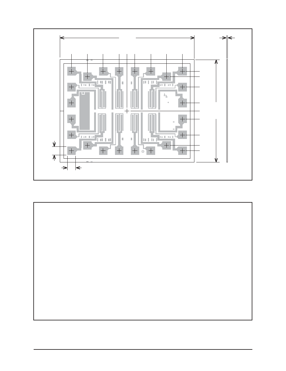
THAT 380G
GKH
Y
K
TH
A
T
31
2
17
C
1
18
B
Q1
E
Q1
B
Q1
C
Q3
C
Q3
B
Q3
E
Q5
E
Q5
B
Q5
C
Q7
E
Q7
B
Q7
C
Q2
C
Q2
B
Q2
E
Q8
C
Q8
B
Q8
E
Q4
B
Q4
E
Q6
E
Q6
B
Q4
C
Q6
C
Q1
PNP
Q2
PNP
Q3
NPN
Q4
NPN
Q7
PNP
Q8
PNP
Q5
NPN
Q6
NPN
Fig 1. 380G Die layout
600042 Rev E
THAT Corporation; 45 Sumner Street; Milford, Massachusetts 01757-1656; USA
Tel: +1 508 478 9200; Fax: +1 508 478 0990; Web: www.thatcorp.com
Page 2
THAT380G Transistor Array Die
SPECIFICATIONS
1
Maximum Ratings (T
A
= 25∞C)
Parameter
Symbol
Conditions
Min
Typ
Max
Units
NPN Collector-Emitter Voltage
BV
CEO
I
C
= 1 mAdc, I
B
= 0
36
40
--
V
NPN Collector-Base Voltage
BV
CBO
I
C
=10
mAdc, I
E
=0
36
40
--
V
NPN Emitter-Base Voltage
BV
EBO
I
E
= 100
mAdc, I
C
= 0
5
--
--
V
NPN Collector Current
I
C MAX
10
20
mA
NPN Emitter Current
I
E MAX
10
20
mA
PNP Collector-Emitter Voltage
BV
CEO
I
C
= 1 mAdc, I
B
= 0
≠36
≠40
--
V
PNP Collector-Base Voltage
BV
CBO
I
C
= 10
mAdc, I
E
= 0
≠36
≠40
--
V
PNP Emitter-Base Voltage
BV
EBO
I
E
= 100
mAdc, I
C
= 0
≠5
--
--
V
PNP Collector Current
I
C MAX
≠10
≠20
mA
PNP Emitter Current
I
E MAX
≠10
≠20
mA
Collector-Collector Voltage
BV
CC
±100
±200
--
V
Emitter-Emitter Voltage
BV
EE
±100
±200
--
V
Operating Temperature Range
T
A
0
70
∞C
Maximum Junction Temperature
T
JMAX
150
∞C
Storage Temperature
T
STORE
-45
125
∞C
NPN Electrical Characteristics
2
Parameter
Symbol
Conditions
Min
Typ
Max
Units
NPN Current Gain
h
fe
V
CB
= 10 V
I
C
= 1 mA
60
100
--
I
C
= 10
mA
100
--
NPN Current Gain Matching
Dh
fe
V
CB
= 10 V, I
C
= 1 mA
--
5
--
%
NPN Noise Voltage Density
e
N
V
CB
= 10 V, I
C
= 1 mA, 1 kHz
--
0.8
--
nV
÷Hz
NPN Gain-Bandwidth Product
f
T
I
C
= 1 mA, V
CB
= 10 V
350
MHz
NPN
DV
BE
(V
BE3
-V
BE4 ;
V
BE5
-V
BE6
)
V
OS
I
C
= 1 mA
--
±0.5
±3
mV
I
C
= 10
mA
--
±0.5
mV
THAT Corporation; 45 Sumner Street; Milford, Massachusetts 01757-1656; USA
Tel: +1 508 478 9200; Fax: +1 508 478 0990; Web: www.thatcorp.com
600042 Rev E
Page 3
1. All specifications subject to change without notice.
2. Unless otherwise noted, T
A
=25∞C.
SPECIFICATIONS
1
(Cont'd)
Parameter
Symbol
Conditions
Min
Typ
Max
Units
NPN
DI
B
(I
B3
-I
B4,
I
B5
-I
B6
)
I
OS
I
C
= 1 mA
--
±500
±1500
nA
I
C
= 10
mA
--
±5
nA
NPN Collector-Base Leakage Current I
CBO
V
CB
= 25 V
--
25
--
pA
NPN Bulk Resistance
r
BE
V
CB
= 0 V, 10
mA < I
C
< 10 mA
--
2
--
W
NPN Base Spreading Resistance
r
bb
V
CB
= 10 V, I
C
= 1 mA
--
30
--
W
NPN Collector Saturation Voltage
V
CE(SAT)
I
C
= 1 mA, I
B
= 100
mA
--
0.05
V
NPN Output Capacitance
C
OB
V
CB
= 10 V, I
E
= 0 mA, 100 kHz
3
pF
NPN Collector-CollectorCapacitance (Q3-Q4, Q5-Q6)
C
CC
V
CC
= 0 V, 100 kHz
0.7
pF
PNP Electrical Characteristics
2
Parameter
Symbol
Conditions
Min
Typ
Max
Units
PNP Current Gain
h
fe
V
CB
= 10 V
I
C
= 1 mA
50
75
--
I
C
= 10
mA
75
--
PNP Current Gain Matching
Dh
fe
V
CB
= 10 V, I
C
= 1 mA
--
5
--
%
PNP Noise Voltage Density
e
N
V
CB
= 10 V, I
C
= 1 mA, 1 kHz
--
0.75
--
nV
÷Hz
PNP Gain-Bandwidth Product
f
T
I
C
= 1 mA, V
CB
= 10 V
325
MHz
PNP
DV
BE
(V
BE1
-V
BE2;
V
BE7
-V
BE8
)
V
OS
I
C
= 1 mA
--
±0.5
±3
mV
I
C
= 10
mA
--
±0.5
mV
PNP
DI
B
(I
B1
-I
B2;
I
B7
-I
B8
)
I
OS
I
C
= 1 mA
--
±700
±1800
nA
I
C
= 10
mA
--
±7
nA
PNP Collector-Base
Leakage Current
I
CBO
V
CB
= 25 V
--
≠25
--
pA
PNP Bulk Resistance
r
BE
V
CB
= 0 V, 10
mA < I
C
< 10 mA
--
2
--
W
PNP Base Spreading Resistance
r
bb
V
CB
= 10 V, I
C
= 1 mA
--
25
--
W
PNP Collector Saturation Voltage
V
CE(SAT)
I
C
= 1 mA, I
B
= 100
mA
--
≠0.05
V
PNP Output Capacitance
C
OB
V
CB
= 10 V, I
E
= 0 mA, 100 kHz
3
pF
PNP Collector-Collector Capacitance (Q1-Q2; Q7-Q8)
C
CC
V
CC
= 0 V, 100 kHz
0.6
pF
THAT Corporation; 45 Sumner Street; Milford, Massachusetts 01757-1656; USA
Tel: +1 508 478 9200; Fax: +1 508 478 0990; Web: www.thatcorp.com
Page 4
THAT380G Transistor Array Die
GKH
Y
K
TH
A
T
312
17C
1
18B
*0.021"
0.001
±
* Custom thicknesses are available. Contact THAT Corporation for more information.
1
232
u
1613u
0
95.5
286.5
411.5
477.5
0
95
.5
2
86.
5
4
77.
5
6
68.
5
-95.5
-286.5
-411.5
-477.5
-9
5.
5
-2
86
.5
-4
77
.5
-6
68
.5
90u
90u
Figure 2. Die dimensions
Information furnished by THAT Corporation is believed to be accurate and reliable. However no responsibility is as-
sumed by THAT Corporation for it's use nor for any infringements of patents or other rights of third parties which may
result from it's use.
LIFE SUPPORT POLICY
THAT Corporation products are not designed for use in life support equipment where malfunction of such products
can reasonably be expected to result in personal injury or death. The buyer uses or sells such products for life suport
application at the buyer's own risk and agrees to hold harmless THAT Corporation from all damages, claims, suits or
expense resulting from such use.
CAUTION: THIS IS AN ESD (ELECTROSTATIC DISCHARGE) SENSITIVE DEVICE.
It can be damaged by the currents generated by electrostatic discharge. Static charge and therefore dangerous volt-
ages can accumulate and discharge without detection causing a loss of function or performance to occur.
The transistors in this device are unprotected in order to maximize performance and flexibility. They are more sen-
sitive to ESD damage than many other ICs which include protection devices at their inputs. Note that all of the pins
(not just the "inputs") are susceptible.
Use ESD preventative measures when storing and handling this device. Unused devices should be stored in conduc-
tive packaging. Packaging should be discharged to the destination socket before the devices are removed. ESD damage
can occur to these devices even after they are installed in a board-level assembly. Circuits should include specific and
appropriate ESD protection.